Wednesday 27 July 2016

Moore's law is dead.... or is it?


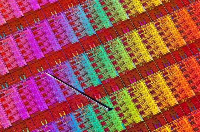
A Haswell processor close up.


If you know anything about processors you will have heard of Gordon Moore. He was the co-founder of Intel and came up with his now famous law.
MOORES LAW : The observation made in 1965 by Gordon Moore, co-founder of Intel, that the number of transistors per square inch on integrated circuits had doubled every year since the integrated circuit was invented. Moore predicted that this trend would continue for the foreseeable future.
This basic observation by Moore has held true since 1965 but things are about to change.  Every year newer and better ways to put transistors on silicon are found. The size of each transistor reduces allowing chip designers to cram more and more in the same size. This basic process has reached its limit. According to the International Technology Roadmap for Semiconductors (ITRS) transistor can't shrink any more. Moores law is dead?
The ITRS—which has been produced almost annually by a collaboration of most of the world's major semiconductor companies since 1993—is about as authoritative as it gets when it comes to predicting the future of computing. The 2015 roadmap will however be its last.
The most interesting aspect of the ITRS is that it tries to predict what materials and processes we might be using in the next 15 years. The idea is that, by collaborating on such a roadmap, the companies involved can sink their R&D money into the "right" technologies.
For example, despite all the fuss surrounding graphene and carbon nanotubes a few years back, the 2011 ITRS predicted that it would still be at least 10 to 15 years before they were actually used in memory or logic devices. Germanium and III-V semiconductors, though, were predicted to be only five to 10 years away. Thus, if you were deciding where to invest your R&D money, you might opt for the iii-V rather than nanotubes (which appears to be what Intel and IBM are doing).
The latest and last ITRS focuses on two key areas :
It will no longer be economically viable to shrink transistors after 2021
What might be done to keep Moore's law going despite transistors reaching their minimal limit.

(Remember, Moore's law simply predicts a doubling of transistor density within a given integrated circuit, not the size or performance of those transistors.)
The first problem has been known about for a long while. Basically, starting at around the 65nm node in 2006, the economic gains from moving to smaller transistors have been slowly dribbling away. Previously, moving to a smaller node meant you could cram tons more chips onto a single silicon wafer, at a reasonably small price increase. With recent nodes like 22 or 14nm, though, there are so many additional steps required that it costs a lot more to manufacture a completed wafer—not to mention additional costs for things like package-on-package (PoP) and through-silicon vias (TSV) packaging.
This is the primary reason that the semiconductor industry has been whittled from around 20 leading-edge logic-manufacturing companies in 2000, down to just four today: Intel, TSMC, GlobalFoundries, and Samsung. (IBM recently left the business by selling its fabs to GloFo.)
The second problem, how to keep increasing transistor density has a couple of likely solutions. First, ITRS expects that chip makers and designers will begin to move away from FinFET in 2019, towards gate-all-around transistor designs. Then, a few years later, these transistors will become vertical, with the channel fashioned out of some kind of nanowire. This will allow for a massive increase in transistor density, similar to recent advances in 3D V NAND memory.
The gains won't last for long though, according to ITRS: by 2024 (so, just eight years from now), we will once again run up against a thermal ceiling. Basically, there is a hard limit on how much heat can be dissipated from a given surface area. So, as chips get smaller and/or denser, it eventually becomes impossible to keep the chip cool. The only real solution is to completely rethink chip packaging and cooling. To begin with, we'll probably see microfluidic channels that increase the effective surface area for heat transfer. But after that, as we stack circuits on top of each other, we'll need something even fancier. Some form of electronics blood, perhaps?
The final ITRS report is a bit of a monster and I have only touched on a few aspects of it. There are large sections on heterogeneous integration, and also some important bits on connectivity (semiconductors play a key role in modulating optical and radio signals).
One interesting piece of short term decision making that will happen very soon is choosing which lithography and patterning techs will be used for commercial 7nm and 5nm logic chips. As you may know, extreme ultraviolet (EUV) has been waiting in the wings for years now, never quite reaching full readiness due to its extremely high power usage and some resolution concerns. In the mean time, chip makers have fallen back on increasing levels of multiple patterning—multiple lithographic exposures, which increase manufacturing time (and costs). Now, however, directed self-assembly (DSA)—where the patterns assemble themselves—is also getting very close to readiness. If either technology wants to be used over multiple patterning for 7nm logic, the ITRS says they will need to prove their readiness in the next few months.
So on the face of it Moore's law looked dead but there are a number of new techniques and technologies waiting in the wings that may well allow us to get round the current limitations. Time will tell.

An "EPIC" journey.

An “EPIC” journey beyond the standard.


AAEON goes on an “EPIC” journey beyond the Standard.


EPIC: An Introduction
In 2004, the PC/104 Embedded Consortium released the standard for Embedded Platform for Industrial Computing, more commonly referred to as EPIC. This standard for SBCs was intended to fill the gap that existed between the small, stackable PC/104 solutions and the larger EBX solutions. According to the PC/104 Embedded Consortium, “the purpose of this specification is to define a physical platform for the mid-sized embedded Single Board Computer (SBC) with multiple I/O expansion options. Its size is midway between the industry standard PC/104 stackable format and EBX SBC format. The added space allows for combining features on an SBC which would normally be found on multiple PC/104 modules”


As noted by the PC/104 Consortium, the EPIC standard defines a board that has x and y dimensions well- suited for smaller embedded industrial PC systems. With more board level real estate, EPIC systems can accommodate greater I/O integration as compared to its sister PC/104 standard that would require more stack-on peripheral boards. The dimensional increase also allows for the use of higher performance processor that often call for advanced heat dissipation. Take note of this issue of heat dissipation.

Reduced Total Cost of Ownership AAEON’s EPIC products are fully tested for compatibility and equips a comprehensive set of core functionalities that render additional modules unnecessary (less expansion), effectively lowering the total cost of ownership (TCO) by 10 ~ 20%.
Legacy I/Os Expandability In computing, looking back is as important as looking forward. In that regard, AAEON’s EPIC products are designed to support legacy systems with the inclusion of the PC/104, PCI-104 (or PCIe) for prolonged use of tried-and-true systems while future-proofing it with newer, more modern technologies.

CPU Solder up Design
Since the Cedar View platforms, aka EPIC-CV07, EPIC-BT07, EPIC-QM77, EPIC-BDU7, AAEON’s EPIC products have boosted the “Solder up” design that places the CPU at the solder side of the PCB. Aiming to take the hassle out of thermal management, the design allows users to adopt a broader range of coolers (even making the idea of treating the chassis as a heat sink possible) without altering the layout of the components, saving development and system integration costs.


Wide Voltage Solution
Depending on the situation for which the solution is deployed, voltage can be a major hurdle to overcome. With this idea in mind. AAEON’s EPIC products are built to support a wide voltage range of 9-24V design to reduce the possibility of damaging the onboard components in the event a DC to DC converter module is used. In addition, the extended voltage range grants enhanced adoptability as up to 80% of today’s industrial requirements can be adequately satisfied, without the need for additional power modules. Flexible System Assembly 
The EPIC standard is exceptionally well-suited for smaller embedded industrial PC applications with its generous dimensions, offering a compact system with I/Os most conducive in today’s industrial use. AAEON’s EPIC board offers has on them up to six USB ports (USB 2.0/ 3.0), eight COM ports (RS-232/422/485), and two Mini-PCIe slots to satisfy the needs for extra components without assembling additional I/O modules.


“EPIC” Technology in Action The AAEON family of EPIC SBCs offers a line of versatile solutions. These highly integrated SBCs can be found serving the requirements of various industry segments from mobile infotainment to industrial automation, and even in the retail space. Due to the fact that AAEON has made these EPIC SBCs much like a component in terms of mechanical and thermal consideration, the benefits they bring to application developers are truly “EPIC” and considerably minimize the limitations for implementation.

EPIC-SKS7 The EPIC-SKS7 is the latest and most advanced member of AAEON’s EPIC product family with a 6th Generation Intel® Core™ processor. The enhanced performance delivered by the chips came in form of support for up to 16 GB of DDR4 memory and clearer, higher resolution video output, making it viable in demanding applications such as high resolution machine vision equipment or mini-servers. The board also sports a CPU socket allowing for greater flexibility.

EPIC-BDU7
Based on the Broadwell platform, the EPIC-BDU7 carries a U-series CPU that lowers power consumption to 15 W, while still delivering impressive performance for 4K resolution media content or triple independent displays. The abovementioned solder up design is featured on this board in addition to the inclusion of the PCI-104 interface, two features that place the board in an ideal position for applications where legacy systems are in place and convenient thermal management is required, namely industrial automation and certain military equipment.


EPIC-BT07 While the Intel® Core™ series is deemed overpowered for certain applications, such as industrial HMIs, the EPIC-BT07 will be up to the task with its lower grade, but less power hungry Intel® Atom™ CPU. Still sporting a solder up design, the board is capable of dual displays as well as wide voltage support of 9 ~ 24V with a healthy set of I/Os, including six USB ports, two RJ-25 ports, and as many as six COM ports. Similar to its Broadwell counterpart, the EPIC-BT07 also uses a fanless thermal solution.

EPIC-CV07 & EPIC-QM57 The most mature and seasoned platform among the AAEON EPIC product family, the EPIC-CV07 and EPIC-QM57 have been the staples of the product line and ideally suited in applications ranging from industrial machinery to intelligent transport. Support for legacy systems are highlighted with the boards’ PCI-104 and PCIe interface as well as older operating systems such as Windows XP. In addition, the EPIC-CV07 carries as many as eight COM ports while the EPIC-QM57 sports a CPU socket for greater flexibility. 


About AAEON AAEON is a leading manufacturer of advanced industrial and embedded computing platforms. Committed to innovative engineering, AAEON provides integrated solutions, hardware and services for premier OEM/ODMs and system integrators worldwide. Reliable and high quality computing platforms include industrial motherboards and systems, industrial displays, rugged tablets, PC/104 modules, PICMG half-size and full-size boards and COM modules, embedded SBCs, embedded controllers and related accessories.

AAEON also offers customized end-to-end services from initial product conceptualization and product development on through after-sales service programs. 

AAEON is a GSA contract holder (#GS-35F-0470Y) serving the Federal, State & Local government sectors. AAEON is also an Associate member of the Intel® Internet of Things Solutions Alliance. From modular components to market-ready systems, Intel and the 400+ global member companies of the Alliance provide scalable, interoperable solutions that accelerate deployment of intelligent devices and end-to-end analytics. Close collaboration with Intel enables Alliance members to innovate with the latest technologies, helping developers deliver state-of-the-art, first-to-market solutions. 


More information can be found regarding all of AAEON’s product lines at http://www.review-displays.co.uk or call us on 01959 563 345


Tuesday 12 July 2016


AMT releases Ruggedized T-Model PCI Touch Solution
Projective capacitive (PCAP or PCI) touch enabled systems designed to handle a large volume of users, installed in high foot traffic areas, or subjected to rough handling often require a tough ruggedized PCI touch surface more protective than standard thickness glass. As the leading provider of touch panels to the industrial, medical, and commercial fields, AMT has developed a ruggedized PCI product in our new T-Model series PCI touch solution. T-Model PCI touch panels can utilized a cover lens thickness of 6mm.
Touch systems operated by the public or in the field may be expected to handle large numbers of input actions, be operated much more callously than personal electronics, or be subjected to impact by stray objects. The countless motorists passing through a gas station have little reason to treat the touch enabled gas pump gently when rushing on their way. Similarly, kiosk and point of sale terminal operators concentrate on completing appoint tasks instead of the machinery's wellbeing. All these systems must be tough enough to not just withstand the continuous impact of fingers but also the misplaced gas nozzle, errant handbag, or unguided shopping cart. In order to meet these applications requirements, a system designer designing a PCI touch panel with a ruggedized glass surface will, in general, consider utilizing a glass panel from 4mm to 6mm thick.
Ahead of this demand, AMT has released its T-Model series of firmware for PenMount PM1310/1410/1710/1711 controllers for the construction of ruggedized PCI touch panels. Customers can select AMT standard stock PCI touch panels from 8.4" to 24" to be outfitted with thick glass. AMT's T-model PCI touch solution provides increased durability by allowing the lamination of décor glass of 6mm thickness to standard medium and large size AMT PCI sensors. Décor glass lamination service can be provided by AMT or competed at the customer end. The T-Model firmware update is then required for thick cover lens touch operation with support for standard glove types. If you already possess an AMT OCA-Film-Film (AFF) sensor and can add the appropriate thickness décor glass, we can provide you with the firmware update per your request. All PCI sensors and PenMount PCI touch control boards used will be current models, with the only changes being cover glass thickness of 6mm and PenMount controller firmware. Of course, if 4mm or 5mm glass is selected for use with the T-Model PCI solution, we will adjust and provide custom firmware to suit your needs.

At AMT, we prioritize the ability to anticipate customer needs. We provide total touch solutions tailored to customers' application environments and system requirements. These solutions are robust, reliable, and easy to integrate without the need for complex adjustment, tuning, or calibration. If you are designing a ruggedized system, AMT's T-Model PCI solution may be suitable for you. Please contact RDS on 01959 563 345 for more details.

www.review-displays.co.uk